


Introduction
Debugging embedded communications is one of the most common tasks for electronic design engineers. Efficient Analysis of serial communications requires more than simple triggering and decoding but historically there has been a significant cost difference between the oscilloscopes with mixed signal, serial triggering, and serial decode capabilities and the high performance instruments with advanced analysis. Engineers need the ability to test long term signal quality characteristics including jitter and eye patterns without investing in high performance, high cost solutions.
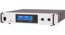
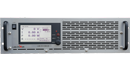
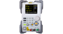
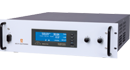
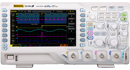
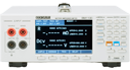
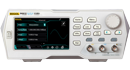
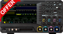
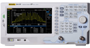
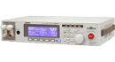
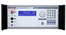
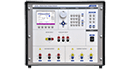
The MSO8000 (Figure 1) provides the most complete analysis capabilities, deepest memory, and highest sample rate in its class. Built for embedded design and debug, the MSO8000 is designed to enable engineers to speed verification and debug of serial communications on a budget. Let’s look at how class leading sampling, memory, and analysis can be used debug complex signal quickly and easily with the help of Jitter and Eye Analysis.
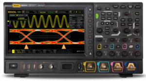
Figure 1: The MSO8000 High Performance Oscilloscope
Characterizing Jitter
Clock precision is critical to high performance digital data transmission. Subtle changes in clock frequency affect error rates and data throughput, but these timing errors can’t be visualized easily in a traditional oscilloscope view. Jitter analysis can be done on these types of signals. Utilizing the high sample rate and the deep memory, the oscilloscope compares the changes in time between thousands of clock transitions. This makes it possible to visualize timing fluctuations below 100 picoseconds while also tracking changes in clock timing over long time periods.
One of the keys to visualizing jitter is the TIE or Time Interval Error. The Time Interval Error is the difference in time between the occurrences of the expected and the actual clock edge. There are two main visualization tools we use with TIE for debugging. First, is the TIE trend graph. This shows the accumulated error in time of the TIE values. This trend is a valuable debug tool since it highlights periodic types of jitter. Figure 2 shows the high speed clock signal on channel 1 (yellow) and the TIE Jitter trend in purple. The vertical axis units for the TIE trend shown here is 10 nanoseconds per division. The trend shows that the jitter TIE accumulates periodically. That implies a periodic signal or event is affecting the clock frequency. Next, investigate the TIE trend with measurements or cursors as shown in Figure 3. The cursors make it easy to view the period of the signal and calculate the frequency as well (1/DX). Direct measurements of the TIE Trend can also be made. The period of these changes are an important clue as to the root cause of any jitter issues.
In addition to the TIE trend you can also calculate the distribution of the TIE values. The shape and standard deviation of the TIE values is an important component of determining root cause. For the signal above the histogram is shown in Figure 4.
When using the TIE trend and distribution to debug and solve jitter related issues it is important to understand the nature of the TIE values and trend. Remember, that TIE is calculated as the accumulated changes in the period of the underlying signal. This means that the TIE graph looks like the integral of changes in the period. Therefore, the triangle wave shown in the figures so far represent a square wave change in the period. This is critical to understanding how to debug signal jitter. The TIE trend shows the period changes lengthening linearly (triangle rising) and then the period changes shortening linearly (triangle falling). When TIE is increasing linearly, the period must be longer than the expected period, but at a fixed value since the sum is linear. When TIE is decreasing linearly, the period is at a fixed value shorter than expected. Therefore, the period is changing between 2 fixed values at this frequency. One is just above and one is just below the expected period. We are therefore looking for a 10 kHz square wave that is somehow affecting our clock timing. We can learn from the histogram that this fluctuation appears to be constant as the TIE distribution is evenly and symmetrically spread across those values.
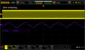
Figure 2: TIE trend graph showing periodic jitter
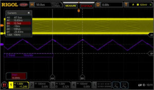
Figure 3: TIE trend graph cursor measurements
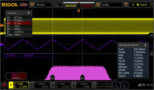
Figure 4: TIE trend and TIE Histogram
After testing different nearby signals on our device under test, we find a time correlated square wave (Figure 5) shown in blue at that frequency that is affecting our serial clock timing.
Jitter can often be caused by issues with PLLs, power fluctuations, or emissions, among others. Let’s look at some use cases where the histogram data is important to correct jitter analysis.
Figure 6 shows a bimodal distribution of the TIE values in the histogram with a sinusoidal TIE trend. Here we can see the standard deviation (sigma in the histogram statistics) is about 3.2 ns. Since these trends have a mean value of close to zero, the standard deviation can also be approximated as the RMS value of the signal (shown in the RMS measurement in the bottom left). Since both sinusoidal waves and triangle waves have an integral that appear visually sinusoidal it can be difficult to discern whether the underlying changes to the clock period are more triangular or sinusoidal. The standard deviation and the histogram are additional tools that can help to determine what signals might be interfering. Often, signal timing shows a sharper correction or snapback to the nominal timing as the clock is realigned. Visually this can look like more of a ramp or saw wave. The histogram can help to visualize the asymmetry if the signal drifts slowly and then is corrected quickly. Figure 7 is a good example of an asymmetrical jitter distribution that still appears nearly sinusoidal in the jitter TIE trend. A distribution like this makes it easier to pinpoint the process that might be causing the fluctuations.
One important key to jitter measurements is to remember that this is about data integrity and ultimately about errors that cost the system time or bandwidth. In other words, it isn’t just about how much the timing might fluctuate but how your receiver views the data. For this reason it is important to test the signal for jitter in the way that the receiver is also determining the clock settings. In serial communications the clock can be explicit, meaning that there is a clock line transmitted for this purpose. There may also be a constant clock speed defined by the communication standard. It is also common for the receiver to ‘recover’ the clock from the signal itself using a PLL circuit.
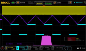
Figure 5: Finding root cause with Jitter analysis
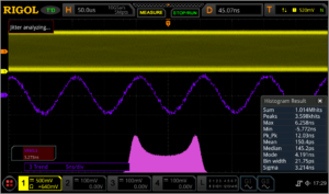
Figure 6: Standard Deviation of the histogram
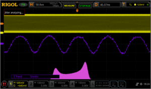
Figure 7: Asymmetry in the histogram results
The design of the receiver has an outsized effect on jitter and timing. If the receiver uses a constant clock rate at a 70 Mb/sec rate the jitter appears as shown in the figures above. If the receiver uses a 1st order PLL with 200 kHz of bandwidth it can eliminate much of the low frequency jitter we saw at 10 kHz. This is shown in Figure 8. The MSO8000 can emulate explicit, constant, 1st order PLL, and 2nd order PLL clock recovery systems to precisely measure the jitter or eye diagram as it will be seen by the receiver. These are important capabilities to accurately debug critical timing issues and ignoring insignificant issues. Once we are correctly emulating the clock recovery and have removed key causes of jitter, we can zoom in on the TIE Trend to 500 picoseconds per division (Figure 9). We still see some periodic fluctuations but they have been reduced significantly and may no longer have any impact on the bit error rate. Once, all the jitter has been adequately addressed in the system you can view noise sources below 500 picoseconds per division as shown in Figure 10. The MSO8000 Oscilloscope also enables a direct statistical table view of the TIE values as well as Cycle to Cycle values and values calculated from both the positive and negative widths. Together, these jitter tools make it possible to carefully visualize and analyse timing issues in vital serial communication links.
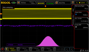
Figure 8: Dynamic Clock Recovery
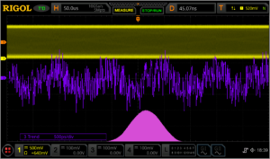
Figure 9: Remaining Jitter
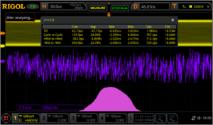
Figure 10: Jitter Measurements
Signal Quality & the Eye Diagram
Timing is only one of the characteristics that contribute to overall signal quality. The goal of all signal quality analysis is to reduce data error in the transceiver link. Errors are often caused by timing and clock issues, but problems stemming from bandwidth, grounding, noise, and impedance matching all can impact how a bit is interpreted by the receiver. The best method for visualizing the holistic data signal quality is the eye pattern or eye diagram test. Real-time eye diagrams are a great way to validate and debug serial data links where throughput and bit error rate are important to system performance.
The eye diagram analyses the data line aligning the bit timing with the recovered clock. The same clock recovery options are available here as in the jitter toolkit. They eye diagram is then created by lining up and overlaying each bit. A density plot is then created from what can be thousands of bit sequences. This is called an eye pattern or eye diagram because the shape in the center resembles an open eye that closes to a point on each side. The goal is to have an open eye where the bit level (0 or 1) is correctly interpreted at the center of the eye.
The eye pattern in Figure 11 shows some potential issues. Depending on the user settable thresholds, the instrument calculates the width and height of the eye. This signal has a bandwidth limitation. We can interpret that because the slope of the rising and falling edges on each side of the eye is not as steep as our design planned for. Analytically, we can determine this by comparing the eye height, eye width, and signal risetime on the screen to our design documents. There also appears to be some frequency uncertainty with regard to the recovered clock. We can see from the histogram that the distribution of the period is not Gaussian implying some non-random causality to the frequency shifts. Lastly, there is some noise causing the amplitude to fluctuate. This closes the eye vertically.
Using the eye diagram as a visual debug tool, evaluate the cables and connections. Also, look for layout, cross-talk, or other emissions that might be impacting signal quality. Once we remove the signal causing the frequency fluctuations we see the eye start to open in Figure 12. The purple histogram now shows that the remaining timing errors are at least symmetrical. This also improves the eye width in the eye measurements window.
Figure 13 is the result once we identified and removed the nearby noise source. This improves the eye height and width and the entire signal is more precise. Now it is clear that the rising and falling bit transitions don’t reach the same high or low level as the non-transitioning bits. We also see that the rising and falling edges themselves have about a 45° slope with these time and voltage settings. The design document indicates that this should be higher. This is likely a bandwidth issue that is both limiting the risetime of the transitions and causing the eye to close vertically when the signal does not return all the way to its peak or base by the middle of the bit.
Finally, Figure 14 demonstrates improved bandwidth after changing our transmitter circuit. The histogram distribution shows that this has also removed some of the outliers in the signal timing. The improved bandwidth shows clearly in the improved Risetime as well as a completely open vertical eye.
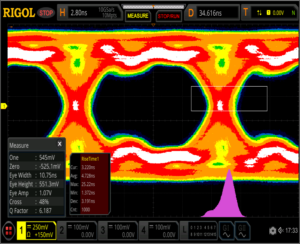
Figure 11: Eye Diagram of signal causing errors
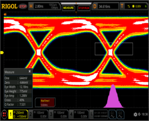
Figure 12: Eye Diagram with improved timing
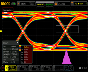
Figure 13: Eye Diagram with improved noise
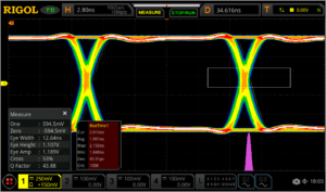
Figure 14: Eye Diagram after debugging and improvements
Conclusions
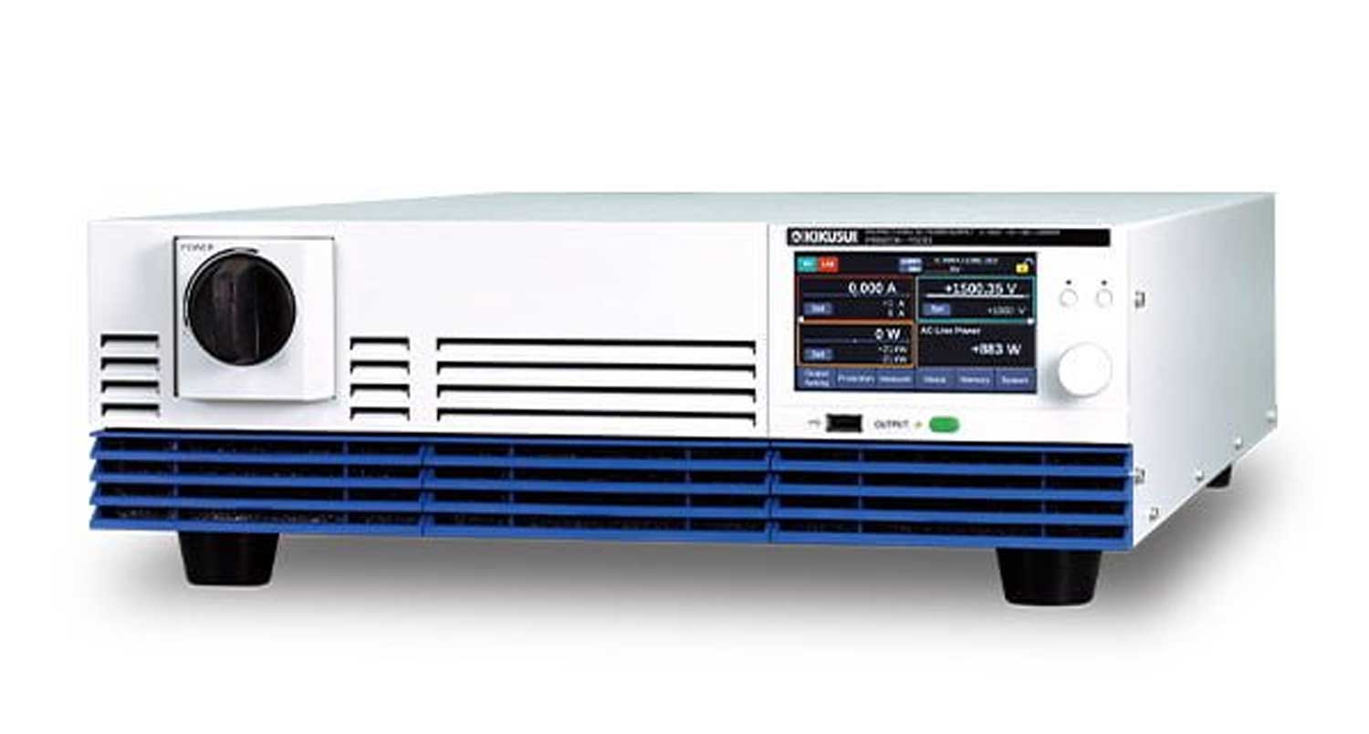
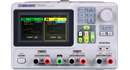
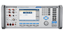
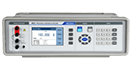
Embedded design and debugging of digital data is a critical requirement in modern electronic products. Modern high performance digital oscilloscopes expand the analysis capabilities available to the everyday engineer’s bench. RIGOL’s UltraVision II technology and our MSO8000 Series oscilloscopes (Figure 15) complete these tools with jitter and eye diagram analysis options making complete signal quality analysis affordable and easy to use. Jitter and eye diagram analysis on the MSO8000 simplifies viewing, analysing, and resolving issues involving timing, noise, bandwidth, and overall signal quality in serial data links. With new analysis capabilities built on the deep memory and high sample rate of the UltraVision II platform, RIGOL’s MSO8000 Series oscilloscopes are the high performance debugging tool of choice for today’s embedded engineer.

Figure 15: The MSO8000 High Performance Oscilloscope
Products Mentioned In This Article:
- MSO8000 Series please see HERE